Definition of "Free Integrated Circuits" :
It's the same meaning as for Free Software, but for Integrated Circuits / Electronic components.
It is not to be confused with "Free Hardware" that usually refers to "Free PCB Boards" (The schematic of the board, and its processed, placed and routed equivalent PCB Layers) which are Free in terms of board schematic and routed PCB, but always made out of non-free electronic components. Indeed the wording "Free Hardware" is bad, because it tends to let users understand that the whole device hardware is free, while only its PCB is free, not all the components it is made of. This confusion is obviously serving cyber-imperialist goals of the Empire or competitors as it is greatly contributing to mask the "Free Integrated Circuit" problem and needs. "Free Hardware" is therefore a terminology with political and geopolitical fascist and imperialist bad consequences : It opens an avenue to the huge lie by omission that "Free Hardware" gives end-users full knowledge and control over its electronic devices, while it actually gives the user only a superficial, top level control over its electronic devices at PCB board level, not at integrated circuits levels.
That being said, creating truly fully free integrated circuits or electronic components in general is a way more complex task that the ones needed for free software. I propose to examine in details the different aspect of free software, and have a look at their equivalency for free integrated circuits :
TO DO : Insert a few paragraphs on free software main mandatory characteristics and their equivalency for free integrated circuits.
We can conclude from previous paragraphs that it is way more complex in terms of implementation to offer the same kind of freedom guarantees offered by Free Software :
- Source code (VHDL) or schematic available to end-users for peer review and understanding how it works and how to use it and integrate it into designs.
- Source code or schematic publish under a GPL licence or equivalent.
- Free Software Tools available to compile the VHDL source code or process the schematics and generate the typon of each layer that will physically instantiate the targeted design IC, "the chip", and ensure & check that all those typons IC layers do implement exactly what was specified in the source code or schematic, and feed these typons to a fab so that the IC Chip can be manufactured. These typons for each IC layers are to be seen similarly as PCB layers for a PCB.
- The need of a Free Standard Cells Library published under GPL or equivalent to instantiate each elementary Logic Gate for digital ICs.
These needs describe above are usually considered by the vast majority of Electronician and IC hackers as sufficient to characterize Free Integrated Circuits. But this is not the case, this is a lie by omission.
So what is missing in this usually accepted definition of Free Integrated Circuits ?
What is missing to offer all the same freedom guarantees as for Free Software is a low cost and simple process, for end-users, is :
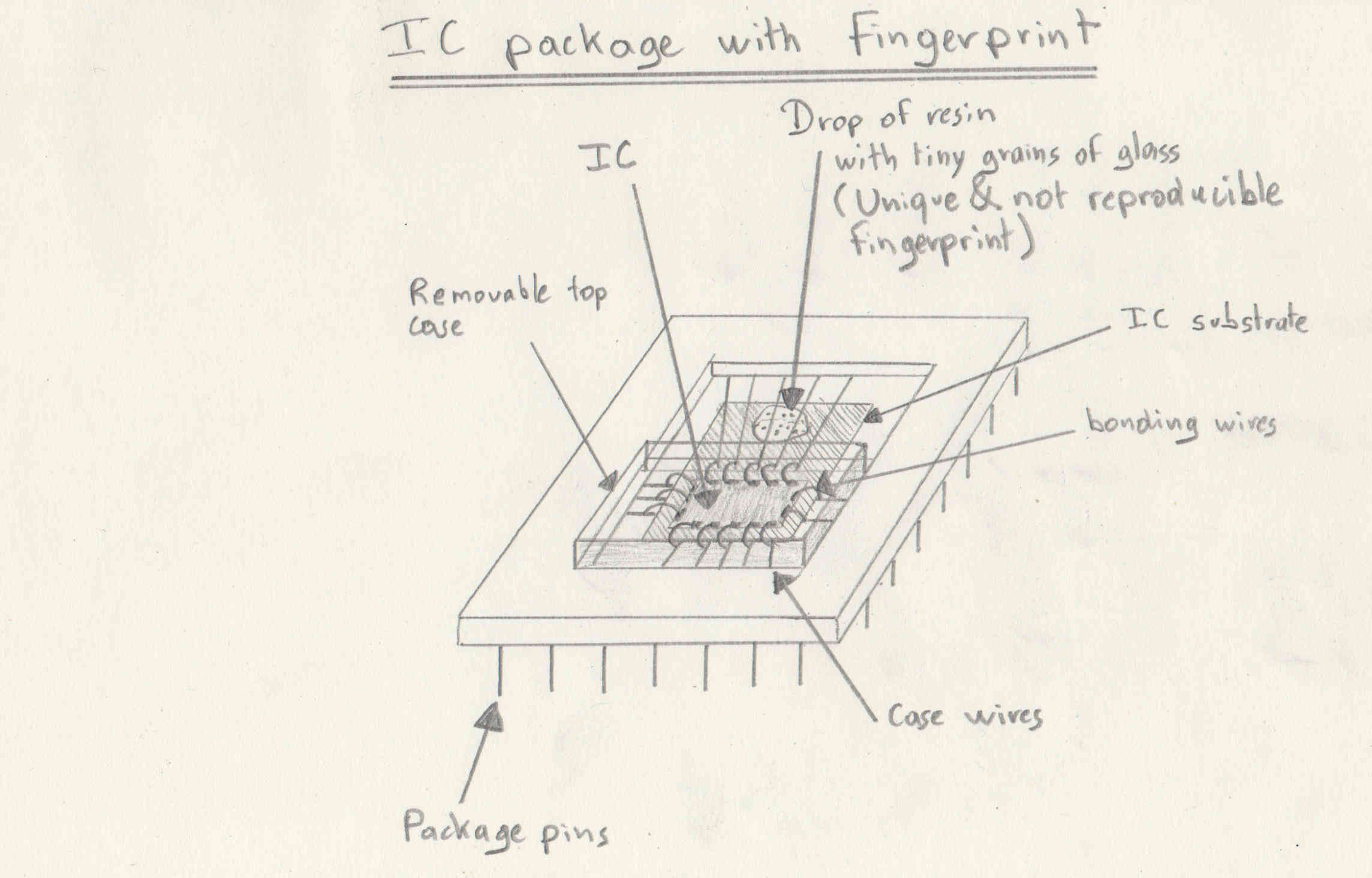
- The ability to simply, safely, non destructively, and as often as needed or desired open the Chip package (Some new packages that can be opened and close as many times as desired by end-users will need to be engineered) so that some low cost tools can later on verify the full integrity or partial integrity of the die it contains.
- Verify the die means verifying that all the layers of the die that is embedded into the package do actually strictly correspond to the ones obtained by compiling the source code / processing the schematics to place and route each elementary logic cell and create the typons for each layer. In other word, the name of the game here is to check that the fab strictly used the same typons as those they were feed with to manufacture the device.
- Verify that each logic gate is actually operational and working normaly (This is needed to mitigate dopant attacks, for example, and to ensure the IC is operational).
- All this need to be doable "in situ" by the end-user himself, with a low cost apparatus that would act like a costly electronic microscope or X-Ray microscope able to see "nanoscale" details. And this is the hard part, because not only there is currently no specific "openable package" standardized, and these is no low cost technology commercialized to scan the die and its different layers like a costly electronic microscope can do, and automate the reconstitution of the full circuitry with all its layers and automatically compare those data to the original ones provided to the fab to manufacture the IC.
Free Integrated Circuits don't exist yet :
This is what can be concluded honestly from the definition above. There is strictly nothing allowing an end-user to check the die integrity of any integrated circuit, no apparatus exist to automate such task, and no "openable" package neither exist or have been standardized. This is clearly a fascist and cyber-imperialist political choice that has lead us to the current situation were we have, as end-users, absolutely no control over "in situ" integrity check of IC.
The best that can be done today :
In order to have an equivalent of Free Integrated Circuits or getting very close from that, we can (Ordered from the less secure but most easy to implement, to the most secure but less easy to implement) :
Use FPGA (There are still no Free FPGA) with free compilation, place and route toolchains, but there are NSA or equivalent backdoors within those FPGA ICs (We know how to mitigate them enough, but it brings a lot of useless additional complexity to the PCB designs). We have free compilation toolchains available (YOSYS) to compile, instantiate, place and route VHDL code, for FPGA or ASICs, but this is the best we can do.
Create ASICs with YOSYS and other free software synthesis tools, using a free Standard Logic Cell library like the one developped by LibreSilicon, but we can't trust the fab who is going to actually manufacture the IC and some backdoors could be inserted covertly by the fab. If no backdoor is inserted by the fab, then we almost have a free integrated circuit, but end-users still can't open the packages and check the full integrity of the circuit : The end-users is still forced to trust the supplier of the IC for being what it should really be. Then, we must understand that we can face post-manufacturing supply chain attacks : Even if the IC produced by the fab is clean and unmodified according to the original manufacturing files (typons) we given to the fab to produce the IC, some supply chain attack can still occure when the fab sends parcels containing these freshly produced IC to you : NSA TAO teams are used, like many other agencies, to intercept parcels, covertly open them, change their contant (Replace the clean ICs with backdoored ones they would have produced covertly). Another problem with ASICs is that if we want to make modifications, the ASIC IC produced become obsolete and must me trashed, they cannot be updated after manufacture. Still, when everything goes right, if the fab is not corrupted, and if we can prevent post-manufacturing supply chain attack for those IC transportation (Transporting them ourselves, physicaly, with our own trusted means, from the fab to the end-users), then we can say that we have free integrated circuit except that the end-users still can't check by themselves we were honest with them : It's still pretty a pretty interesting result, it's very close from full free integrated circuits, and it's much safer that current FPGAs that we know are backdoored.
Implement a design with good old discrete logic (TTL/CMOS) families like the 74xxx families or 4000 families. There are free tools based on YOSYS that can generate PCB Netlist for KiCad using those TTL/CMOS discrete logic gates families, allowing to further place and route them on a PCB from a VHDL source code : Here we can be sure there are no backdoors, if the synthesis tool can be trusted. The end-user can verify the PCB, the design, so here, we have a true operational equivalent of free integrated circuits. The drawback here is the size of the boards, some speed limitations of these discrete logic gates, and ultimately, the design cannot be modified easily when soldered on a PCB, still, it is possible to correct a few bugs the good old way with a few straps and so on.
Implement a design fully hardcoded design on a PCB with discrete logic gates families as above, but without using automated synthesis tools, doing everything manually, the good old way. For many small to medium complexity designs, it's really the best choice as there are no issues of trust with the free synthesis tool.
Doing the same but instead of using discrete logic gates families like those 74xxx or 4000 TTL/CMOS families, we can use discrete transistors. This is the safest, but boards can get rapidly huge, like the number of transistors needed, but it is still an option for small to some medium complexity designs. It can be done with free automated synthesis tools, or manually, the good old way.
Now, I think it is interesting to know that the several 3 last technics in the bullet list can be mixed. Some part of the design that really need the maximum level of transparency and guarantee against backdoors can use a different technics than less important parts. Still the last 3 items in the bullet list normally offer a level of trust almost perfect against backdoors insertion.
The current ICs that are the closest to the definition above are EPROMs thanks to their window that allow some microscopy on the die without destroying the IC, but it's just an optical examination of the die, and no test of each standard cells can be operated.
Crypto-Anarchist Roadmap to obtain truly free integrated circuits :
What we need now is to research and test some end-user simple technics with low apparatus to perform the two main operations that were missing to have those truly free integrated circuits :
- Standardizing new custom "openable" packages for ICs and finding a fab to produce these new packages.
- Researching a fully automated low cost apparatus to perform all the die integrity checking steps, by visual inspection and through micro probes to test each standard cell on the die.
Low cost apparatus for end-users IC full die integrity researches :
This is the biggest part of our collective efforts, and here, we can rely on previous great worl made by a few universities to create cheap nano scale microscopy technics.
The most promising research path is called HS-AFM (High-Speed Atomic Forces Microscopy) which can lead to nano-meter resolution microscopy scan and nano-meter electrical probing (When I say probing, it is the ability to pick up a signal on the die, or to inject a signal on the die at a specific location).
The most interesting work done for HS-AFM is using low cost CD/DVD drives OPU (Optical Pickup Units) (The "optical heads" of a standard CD/DVD player) combined with the precision of low cost cantilevers.
Combining two low cost technologies and technics has been done by a UK university :
https://research-information.bris.ac.uk/ws/portalfiles/portal/319227179/Final_PhD_Thesis_FRP.pdf
And it is giving very promising results : See page 90 of the PDF (Local number page number 60). On page 88 (58) you can see pictures of a cantilever "read" by the laser of an CD/DVD standard OPU.
A CD/DVD OPU costs about $30, and some cantilevers can be found for $300, which is still within the boundaries of what we can call "low cost".
A low cost cantilever supplier :
https://www.budgetsensors.com/standard-tapping-mode-afm-probes
The Tap300-G costs about $300 and would be perfect for our needs.
On the following link, you can read a good article on how OPU are also a loc cost apparatus promising research field for biohacking needs, which is not our primary goal, but still, it is interesting to have a look at this article :
https://pubs.acs.org/doi/pdf/10.1021/acssensors.8b00340